
Graphene to accelerate new developments in nanoelectronics
The Institute for Materials Research at The University of Leeds has brought the UK one-step closer to using graphene in electronic circuits, through the simulation capabilities of the Hartree Centre.
Challenge
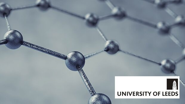
Flexible, strong and an exceptional electrical conductor, graphene has vast potential as an interfacing material that could revolutionise the world of nanoelectronics. Silicon has reached its physical limits, so current research is homing in on techniques to integrate graphene with other two-dimensional materials for use in future nanoscale devices. At an industrial scale, the successful implementation of graphene-based devices relies on a thorough understanding of the material’s quantum mechanical behaviour – which means getting right down to physical interactions at the atomic level. Aberration-corrected scanning transmission electron microscopy (AC STEM) was used at SuperSTEM (also based at STFC’s Daresbury Laboratory) to observe the chemical bonding between metal contacts and graphene. The challenge, however, was to provide a fundamental theoretical explanation of their observations.
Approach
In order to capture the subtle physical mechanisms taking place at the interface, the Hartree Centre provided the group from The University of Leeds with the intensive computational capability required to create accurate simulations. The simulated phenomena gave the scientists increased physical insight, predicting that metal dopants on graphene quickly migrate across the clean regions of the lattice and bond preferentially to edge sites and defects. This confirmed what they had observed using SuperSTEM, and allowed them to understand why it was happening at the atomic level. The results showed that graphene is chemically inert on its pristine regions, but highly reactive on edge sites and defects.
Benefits
A greater understanding of the inner workings of graphene will promote its potential future implementation into nanoelectronic circuits. This piece of work allowed researchers to investigate how metal atoms bind or react with graphene, acquiring a greater understanding of how graphene could work with the metal contacts in electronic devices. Industrial applications of this research include the potential for increasingly faster nanoelectronic technology in any device that uses a transistor, with researchers also looking into potential applications for graphene in solar cells. Speed is an ongoing priority in the technology sector, since faster devices are often more efficient and provide greater consumer satisfaction. If graphene could be used to create faster circuitry in electronic devices, it could improve the competitiveness of high-tech UK companies and result in an overall boost to the economy.
“The Hartree Centre was vital to the success of our research, without which the project could not have been done – and certainly not the high quality it was. It is particularly useful to have combined access to both the HPC capabilities and computer scientists who can provide support for the optimisation of code, which really enables the machines to be used to their maximum potential. It is also conveniently located alongside SuperSTEM at Daresbury, and a stone’s throw from the new £61m National Graphene Institute in Manchester.”
Andrew Scott, University of Leeds
Join Newsletter
Provide your details to receive regular updates from the STFC Hartree Centre.